Full Deposition | Spot Deposition | ![]() Silica Contamination Wafer Standard for calibration KLA-Tencor Surscan, Hitachi SEM and Hitachi TEM tools |
Silica Contamination Wafer Standard for calibration KLA-Tencor Surscan, Hitachi SEM and Hitachi TEM tools |
Contamination Wafer Standard
A Contamination Wafer Standard is a NIST traceable, particle wafer standard with Size Certificate included, deposited with monodisperse silica nano-particles and narrow size peak between 40nm and 2 microns to calibrate the size response curves of KLA-Tencor Surfscan SP3, SP5 SP5xp wafer inspection systems and Hitachi SEM and TEM systems. This Silica Wafer Standard is deposited as a FULL Deposition with a single particle size across the wafer; or deposited as a SPOT Deposition with 1 or more particle size standards precisely located around the wafer.
Particle Wafer Standard, Silica Nanoparticles – Request a Quote
A Contamination Wafer Standard can be deposited as a full deposition or spot deposition on a prime silicon wafer with a narrow size peak of particle size standards. 40 nanometer to 2um particle wafer standards can be provided with 1 or more spot depositions around the wafer with a controlled particle count between 1000 and 2500 per size deposited. Full Deposition across the wafer is also provided with particle counts ranging from 5000 to 10000 particles across the wafer. Silica Contamination Wafer Standards are used to calibrate the size accuracy response of scanning surface inspection systems (SSIS) using high powered lasers, such as KLA-Tencor SP2, SP3, SP5, SP5xp and Hitachi wafer inspection tools. A Contamination Wafer Standard is deposited with silica nanoparticles to calibrate the size response curves of wafer inspection systems using high powered, scanning lasers, such as KLA-Tencor SP5 and SPx. Silica particles are more robust than PSL Spheres with respect to laser energy. The laser intensity of Surface Scanning Inspection Systems, such as Surfscan SP1 and Surfscan SP2 use lower power lasers than the newer KLA-Tencor Surfscan SP3, SP5 and SPx tools, as well as the patterned wafer inspection systems from Hitachi. All of these wafer inspection systems use Contamination Wafer Standards deposited with PSL Spheres or SiO2 particles to calibrate the size response curves of those wafer inspection systems. However, as laser power has increased, the spherical, polystyrene latex particles are found to shrink under high laser intensity, resulting in an ever decreasing, laser size response with repeated laser scans of the PSL Wafer Size Standard. SiO2 particles and PSL Spheres are very close in refractive index. When both types of particles are deposited on a prime silicon wafer and scanned by a wafer inspection tool, the laser size response of Silica and PSL Spheres are similar. Because Silica nano-particles can withstand more laser energy, shrinkage is not a concern with the present level of laser power being used in the KLA-Tencor SP3, SP5 and SPx Surfscan tools. As a result, Contamination Wafer Standards using silica can be used to produce a true particle, size response curve, which is quite similar to PSL Spheres. Thus, calibration of particle size response using Silica particles allows the transition from PSL Contamination Wafer Standards (for the older, lower powered SSIS wafer inspection systems) to a Contamination Wafer Standard using silica nano-particles for the higher powered SSIS tools. Contamination Wafer Standards deposited at 100 nano-meters diameter and above are scanned by a KLA-Tencor Surfscan SP1. Wafer standards below 100nm particle diameter are scanned by a KLA-Tencor Surfscan SP5 and SP5xp
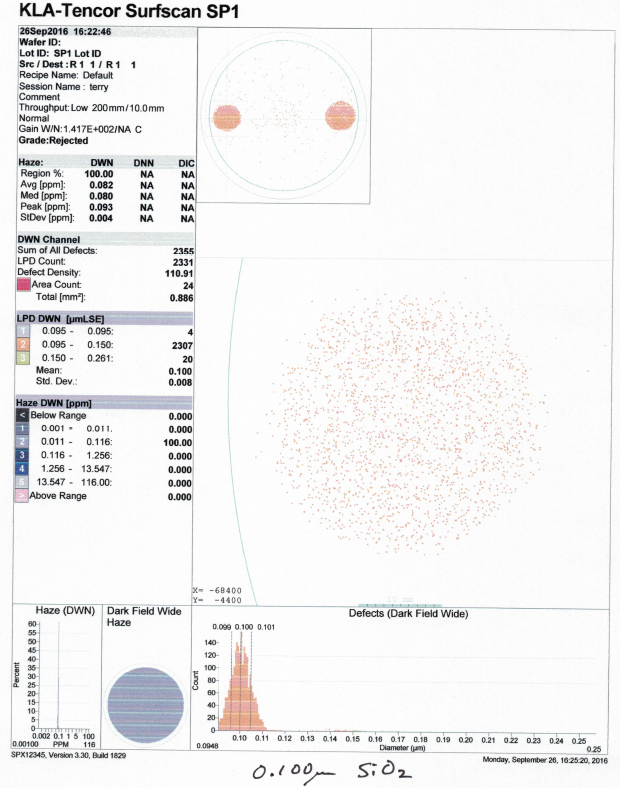
Contamination Wafer Standard, Spot Deposition, 100nm
 |
Contamination Wafer Standards are provided in two types of depositions: Full Deposition or Spot Deposition, shown above.
Silica particles at 100nm are deposited with two spot deposition above.
Full Deposition – Request a Quote
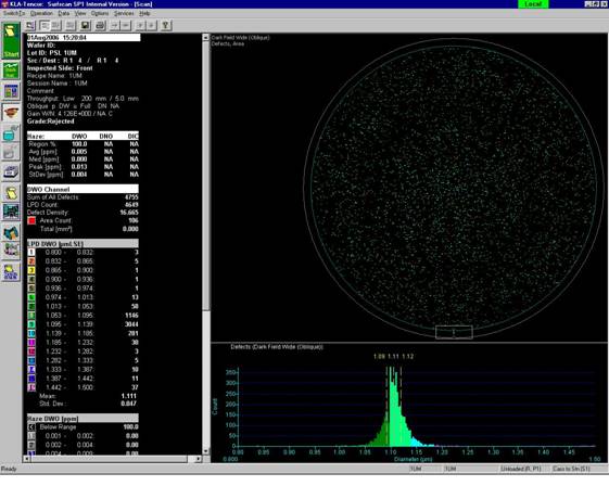
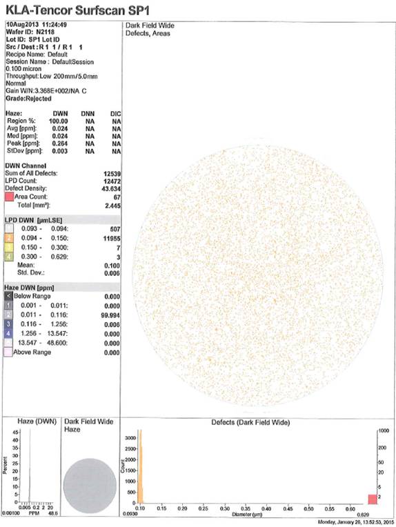
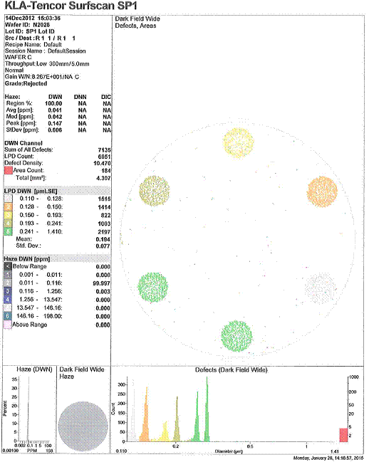
Metrology managers in the semiconductor industry use contamination wafer standards to calibrate the size accuracy of SSIS tools. Metrology managers can specify the wafer size, type of deposition (SPOT or FULL), desired particle count and particle size to deposit. Particle count typically would be 5000 to 25000 count on 200mm and 300mm full deposition wafers; while SPOT Depositions would typically be 1000 to 2500 per size deposited. The Contamination Wafer Standard can be produced as a FULL Deposition with sizes ranging from 40nm to 5 microns. Single SPOT Deposition and multi-SPOT Deposition is also available from 40nm to 5 microns. Spot Deposition Wafers have the advantage of depositing a 1 or more particle sizes on the prime silicon wafer, surrounded by clean silicon wafer surface. When depositing multiple Particle sizes on a single wafer, it is advantageous to challenge the wafer inspection tool across a wide dynamic size range during a single wafer scan and size calibration of your wafer inspection tool. Full Deposition, Contamination Wafer Standards have the advantage of calibrating the SSIS at a single particle size while challenging the SSIS for uniform scan verification across the entire wafer in a single scan. Calibration Wafer Standards are packaged in single wafer carriers and normally shipped on a Monday or Tuesday to arrive before the end of thee week. 100mm, 125mm, 150mm, 200mm, 300mm and 450mm prime silicon wafers are used. 150mm Contamination Wafer Standards or less are scanned using a Tencor 6200, while 200mm, 300mm are scanned with an SP1 Surfscan. A contamination wafer standard, Size Certificate is provided with reference to NIST Traceable Standards. Pattern and Film Wafers, as well as blank photo masks, can also be deposited to create Contamination Wafer Standards.
Contamination Wafer Standard – 200mm, FULL DEP, 1.112 microns

Contamination Wafer Standard, Particle Calibration Standard – 300mm, FULL DEPOSITION, 102nm

Contamination Wafer Standard, 300mm, MULTI-SPOT DEPOSITION: 125nm, 147nm, 204nm, 304nm, 350nm

Contamination Wafer Standard with Spot Deposition – Request a Quote