
Fundamentals & selection
Understand nanoscale terminology, particle morphology, silica-versus-PSL tradeoffs and how to write a requirement that can actually be quoted.
Technical guidance for particle size, material, dispersion medium, surface chemistry, optical response, traceability and semiconductor-metrology applications—published by Applied Physics Corporation.
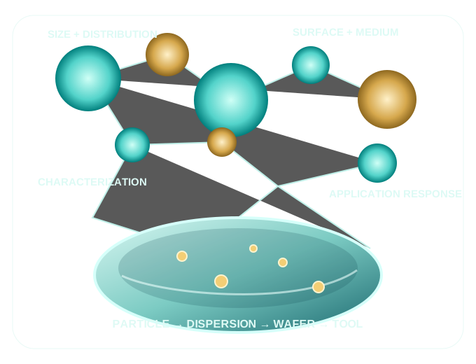
Nominal size is one input. The useful specification also controls distribution, medium, concentration, surface and measurement method.
Two materials with the same nominal diameter can behave differently because they were measured differently, supplied in different media, stabilized at different pH values, functionalized with different surface groups or delivered with different distribution widths.
The fastest route to a useful specification is to define the job first: calibration, optical response, semiconductor inspection, deposition on a wafer, formulation development, surface modification, filtration research or another controlled application. Only then should size, medium, concentration and packaging be selected.
Understand nanoscale terminology, particle morphology, silica-versus-PSL tradeoffs and how to write a requirement that can actually be quoted.
Control medium, dilution, ionic strength, pH, zeta potential, aggregation, storage and transfer losses before they invalidate the intended use.
Separate hydrodynamic diameter from projected diameter, mobility diameter and optical response. Use orthogonal methods when the decision demands it.
Connect silica particle properties to UV/DUV response, wafer-inspection sensitivity, contamination-wafer preparation and SSIS calibration strategy.
Applied Physics currently presents silica families spanning aqueous and ethanol dispersions, dry powders, microspheres, functionalized surfaces and finished contamination-wafer standards. Exact available sizes, concentrations, tolerances, packaging and certification must be confirmed for the requested configuration.
| Method | Typical reported quantity | What it can reveal | Primary blind spot |
|---|---|---|---|
| DLS | Hydrodynamic diameter | Rapid ensemble indication of diffusion behavior and aggregation | Intensity weighting can overemphasize larger populations |
| SEM / TEM | Projected image dimensions | Morphology, primary-particle geometry and direct image-based size | Sampling, preparation and image-analysis choices can dominate |
| DMA | Electrical-mobility diameter | Airborne classification and highly resolved mobility distributions | Requires aerosolization, charge conditioning and method control |
| Zeta potential | Electrokinetic potential | Comparative indicator of colloidal stability under defined conditions | Not a particle-size measurement and strongly condition-dependent |
| Optical response | Scattering or attenuation response | Application-specific detectability and instrument response | Depends on wavelength, refractive index, geometry and instrument model |
Particle response, deposition pattern, wafer substrate and inspection-tool configuration must be treated as one system.
Use wavelength, refractive index, concentration, optical path and detector geometry to define suitability.
Surface chemistry, dispersion energy, loading, viscosity and agglomeration often matter more than the catalog headline.
Research-use materials require explicit boundaries around purity, sterility, endotoxin, functionalization and intended use.
Map application, size, format, medium and surface needs to a defensible family-level recommendation.
Calculate stock and diluent volumes, then apply practical controls for pipetting, mixing and contamination.
Estimate idealized particle counts from size, density, concentration and sample volume—with the assumptions exposed.
Convert nanometers, micrometers and millimeters without shifting orders of magnitude.
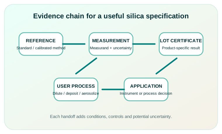
Silica Particle Science is published by Applied Physics Corporation. The site exists to make the selection process clearer, improve the quality of technical inquiries and create durable authority around the particle, wafer and metrology systems Applied Physics manufactures and supplies worldwide.
It does not present itself as an unrelated review site. Product recommendations link directly to the relevant Applied Physics commercial destination, while independent technical sources are cited where they establish terminology, measurement principles or safety controls.
The terms often overlap in commercial use. A useful technical convention is to reserve “nanoparticle” for particles with one or more external dimensions in the nanoscale and use “microsphere” for larger spherical particles, while always relying on the certified nominal diameter and measurement method.
Choose from the application, optical response, density, chemical compatibility, target size, delivery format and required certificate—not from material name alone. Silica can be advantageous for higher refractive-index contrast and semiconductor inspection, while PSL remains common for many particle-counter and aerosol applications.
No. Distribution width, coefficient of variation, morphology, medium, concentration, surface chemistry, agglomeration state, measurement method and uncertainty can all change whether a material is suitable.
Applied Physics offers multiple commercial families and evaluates custom requirements. Feasibility, tolerance, certificate scope, concentration, medium, volume and lead time must be confirmed in a quotation.
Commercial specifications should be confirmed against the current Applied Physics quotation, certificate, lot documentation and product page before purchase or protocol use.
Send the target size, medium, concentration, application, certificate requirements and shipping destination. Applied Physics can evaluate the appropriate silica family or custom pathway.